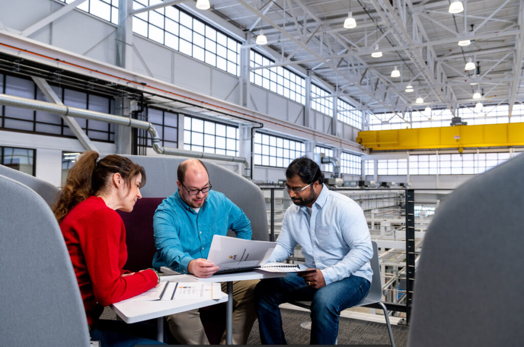
In 2014 as part of a robust New York State economic development initiative called the Buffalo Billion, EWI was selected to establish an advanced manufacturing center in Buffalo, N.Y. After thoughtful planning, Buffalo Manufacturing Works, operated by EWI, opened in April 2015 on the Buffalo Niagara Medical Campus. The team immediately got to work helping innovation-driven organizations excel by partnering with their internal manufacturing, engineering, and R&D teams to deliver better products, grow, and compete.
After just a few years, it became clear that a new, larger facility would be needed as the team grew and additional state-of-the-art equipment was purchased to support the mission.
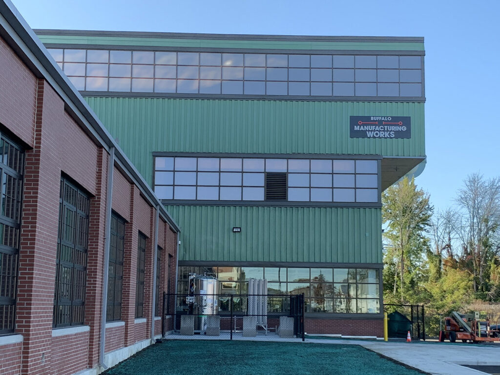
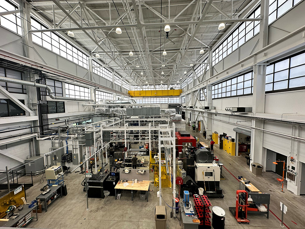
In 2018, Buffalo Manufacturing Works made the move to the Northland campus in East Buffalo, doubling its square footage and joining the Northland Workforce Training Center in anchoring the transformational Northland Beltline corridor.
Northland Campus Overview
Buffalo Manufacturing Works is proud to be one of the anchor tenants in the Northland Beltline redevelopment project that is transforming 35 acres in East Buffalo. The project, supported by a $100 million investment by Empire State Development (ESD), the New York Power Authority (NYPA), and the City of Buffalo, was launched by Buffalo Urban Development Corporation. Our building, located at 683 Northland Avenue, includes the Northland Workforce Training Center, Insyte Consulting, Buffalo Niagara Manufacturing Alliance, Retech Systems LLC, Bank on Buffalo, and World Trade Center Buffalo Niagara.
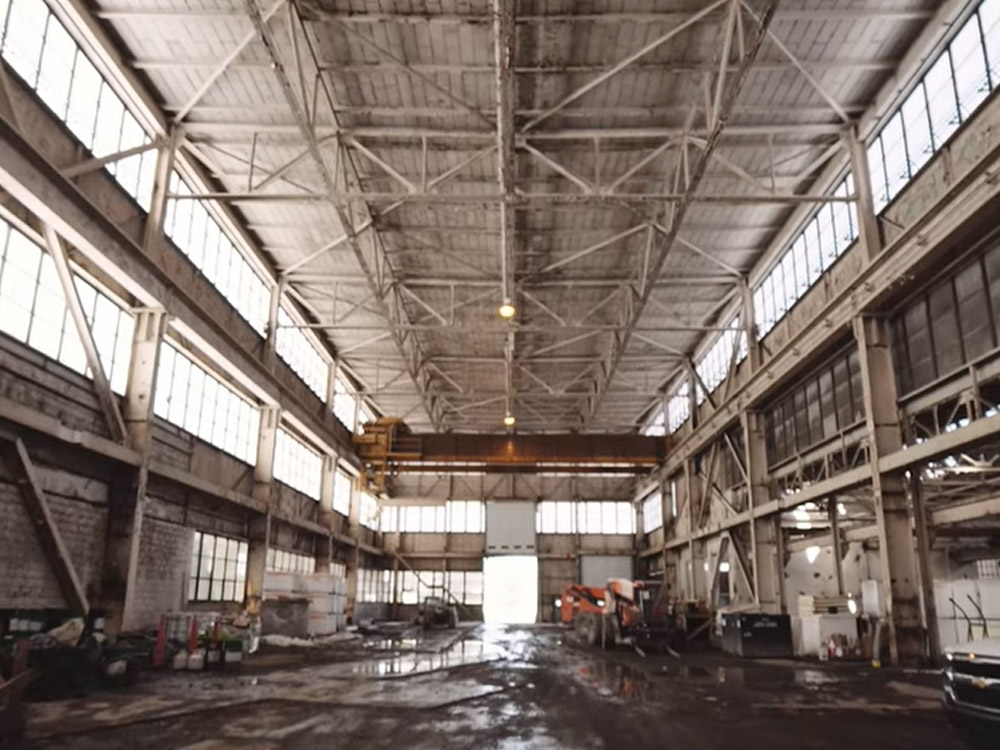
The building was the former home of a WNY manufacturer Niagara Machine and Tool Works complex (founded in 1879) but had been vacant for more than two decades and went through significant renovations to become a state-of-the-art development center.
Shift 2.0
Shift 2.0, a program of Buffalo Manufacturing Works, was established to remove technical obstacles for small to medium-sized manufacturers in Western New York and to enable them to make the most of their limited resources. It offers an accessible and essential first step for those who don’t know how or where to start the process of identifying and investing in achievable and implementable technology.
To help program participants reach the finish line, Shift 2.0 provides access to assessments, trainings, peer learning, and engineering support on certain implementation projects for qualified small to medium-sized manufacturers.
Buffalo Manufacturing Works partners with Insyte Consulting and Launch NY on Shift 2.0. Funding for this program comes from Empire State Development and the Economic Development Administrations’s Build Back Better Regional Community Challenge.
For complete details, visit shiftmfg.com.
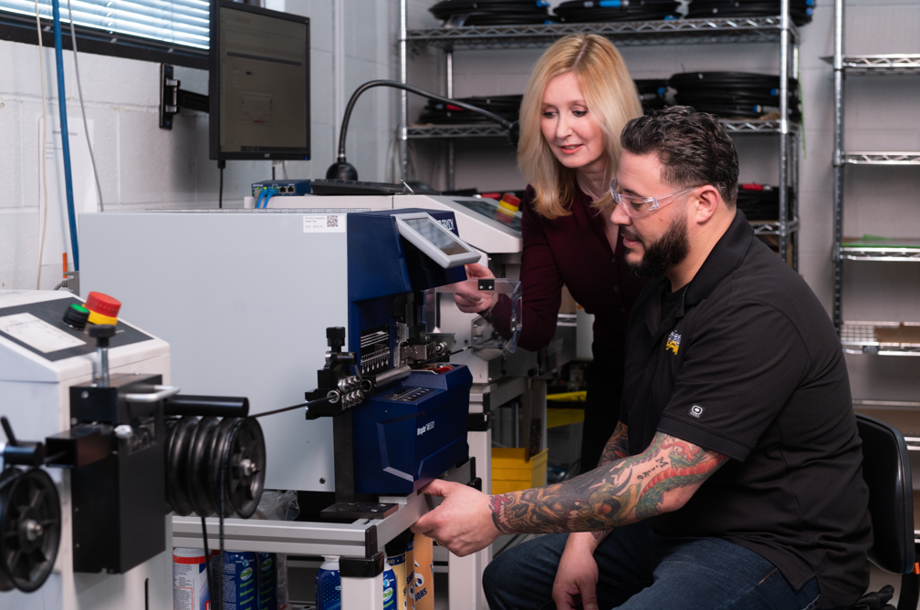
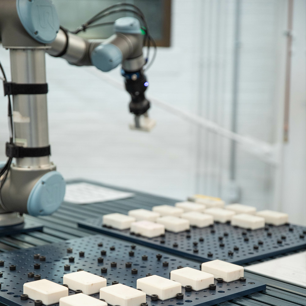
Technologies & Capabilities
The technical team at Buffalo Manufacturing Works works closely with your engineering and manufacturing teams to identify new technologies, then applies them to your products and production processes. Whether you want to lower costs, improve production quality, reduce time to market or increase revenue, our network of experts can steer your business toward greater success. As a division of EWI, we can offer you the full range of technology and capabilities available through our network:
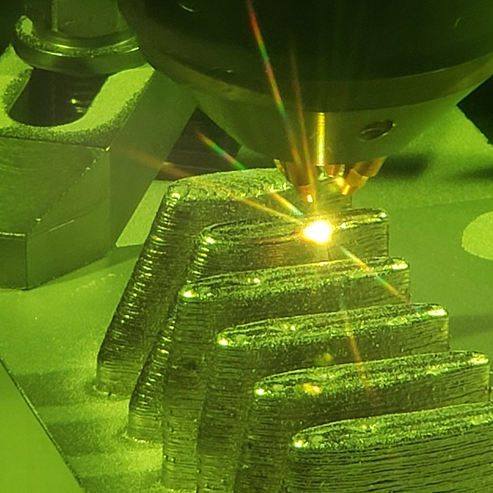
- Additive Manufacturing
- Arc Welding & Directed Energy Deposition
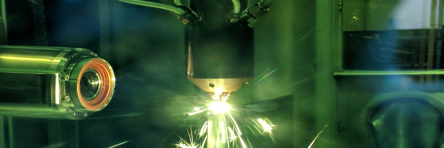
- Laser Processes
- Microjoining
- Plastics Joining
- Resistance Welding & Solid-state Processes
- Ultrasonic Processes
- Advanced Automation
- Forming
- NDE & Inspection
- Structural Integrity & Design
Partners & Funders
As a nonprofit R&D center operated by EWI, our mission is to deliver innovative technical solutions in manufacturing processes that elevate our customers’ competitiveness. We could not do that without the support of many partners and funders who are equally committed to helping manufacturers succeed.
We are grateful for collaboration and ongoing partnership with the following organizations:

Careers
If you’re interested in working at Buffalo Manufacturing Works, check out job opportunities on the EWI careers board. We’re always looking for individuals who enjoy the entrepreneurial thrill of innovation and working as a team to create a satisfying outcome for clients.
To learn about living and working in Buffalo, check out this great Be in Buffalo resource from our partners at Invest Buffalo Niagara.
News and Events
See what’s trending in the world of EWI and Buffalo Manufacturing Works.